Easy to commercialize with enhanced safety
Using molybdenum ditelluride
For the past decades, semiconductor devices were made with the “metal-oxide-semiconductor field-effect-transistor (MOSFET)” method based on silicon that is easy to obtain and cheap to process. However, semiconductors made through this process had high energy consumption and heating problems when applied to artificial intelligence (AI), supercomputer, and Neural Network Processing Unit (NPU) that process huge amounts of data at high speed. Also, as silicon is not structurally flexible, it is difficult to apply it to foldable phones and wearable devices.
To solve these problems, semiconductor industries are focusing on developing new semiconductor devices that are low in energy consumption and high in efficiency as well as flexibility.
Following the trend, Professor Jeong Mun-seok of Hanyang University Department of Physics and his joint research team developed a switching device that is low in energy consumption and high in efficiency compared to existing silicon semiconductors by using a two-dimensional single-material molybdenum ditelluride (MoTe2).
Two-dimensional materials like MoTe2 have unique properties of semiconductors and are evaluated to be applicable in diverse fields due to their high flexibility and transparency.
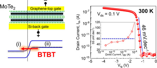
Professor Jeong’s team developed an ultra-low-power “Tunneling field-effect transistor (TFET)” that has enhanced standby power and duty power at room temperature with a subthreshold slope reduced by half using the MoTe2.
The developed TFET has increased safety through the polymer encapsulation structure design, and relatively simple processing is needed when designing as it has a single junction-based structure. Furthermore, it is expected to fully replace previous transistors because the operation is possible at super-high speed.
This research has significance in that the team developed a new structure to lead the TFET industry. Moreover, unlike the usual TFET development with difficulties in automation processing due to complex procedures and lack of safety, Professor Jeong’s transistor is evaluated to have a high possibility of commercialization.
Professor Jeong said that “The recent integrated circuit development was made in terms of efficiency, such as nanofabrication technology development or three-dimensional vertical structure, and the solution was focused on minimizing the energy consumption through data mix and strategic architecture. The fundamental problem is still unresolved. Now is the time when innovative technologies are needed for further development, and this research will be one of the breakthroughs.”
The research (title: Gate-controlled MoTe2homojunction for sub-thermionic subthreshold swing tunnel field-effect transistor) was carried out as a joint research project with Professor Ngoc Thanh Duong of Phenikaa University in Vietnam and was published in the international journal Nano Today (IF=20.722), October edition.